Printed circuit board (PCB) layout is one of the best parts of the project design process. Drawing up schematics, laying out components, and solving the net-routing-puzzle are all fun, oddly relaxing tasks, but my favorite part of PCB design is making them look snazzy. It's as close as this engineer will get to making "art."
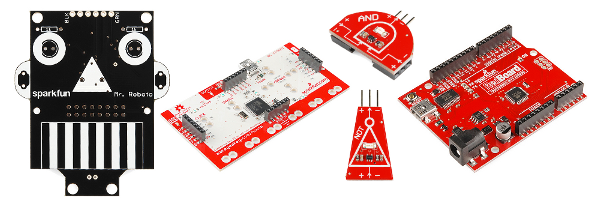
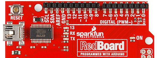
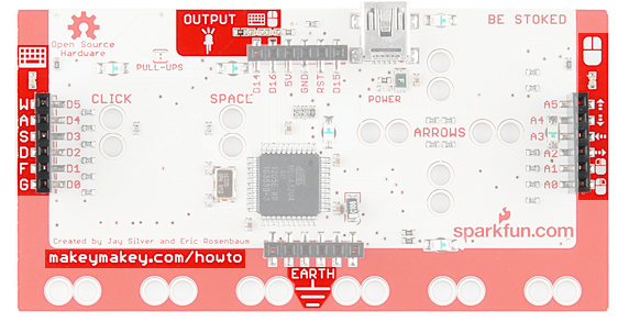
A handful of boards I've had a chance to design with some added flair: Mr. Roboto, MaKey MaKey, LogicBlocks, and the RedBoard.
We do all of our PCB design in Eagle, and we host tutorials, libraries, and classes to help encourage everyone to get their hands on the software and design their own PCB. In my Engineer Thursday blog post I wanted to share some of the PCB art tricks I've discovered through the years of working with Eagle. Hopefully this'll inspire others to have some extra fun with their PCB designs!
Consider the Color Palette
PCB design leaves you with a rather limited color palette: three, maybe four colors to choose from. There's the soldermask, which can be traditional green or (depending on what the fab house can do) SparkFun red, LilyPad/OSH Park purple, Arduino blue, black, yellow, white, orange, or even clear. You'll have two shades of the soldermask to work with: a lighter shade when there's copper underneath, and a darker shade when it's just FR-4 below.
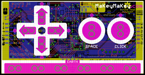
Another, often unused color in your palette is the exposed metal. The color of the metal depends on what you ask for from the fab house. It'll be either silver, copper, or gold. The bare metal can be out of necessity (like the arrow keys on the MaKey MaKey), or completely removed from any net in the schematic (like the ".com" on the top side). In Eagle, to expose metal, you need a layer of copper (top or bottom), with a matching stop layer (tStop or bStop) over that.
Finally, of course, there's silkscreen. Traditionally silk is white, but (again, depending on the fab house) there's also red, blue, yellow, and black. It's even possible to get two different colors of silk on a board. Usually non-white silk colors are an up-charge, but it might be worth it to get the cool-factor you're looking for.
In designing the MaKey MaKey, we tried to make the most of our color palette. There are big blocks of red silk around the borders, carefully exposed white soldermask within the silk, circles and arrows of exposed silver, and little greyish-yellow (soldermask-covered copper) music notes. All painstakingly drawn and layered using Eagle, with the help of a few extra tools.
Eagle Tools
If you've fiddled around with Eagle, you probably know Eagle provides a limited set of tools for drawing basic shapes: the wire tool can draw lines, there's circle and arc drawing tools, and there are the polygon and rectangle tools for drawing big blocks on a layer. The polygon tool is the most versatile of the bunch, you can continue to add vertexes until you've got just the shape you need. That's the tool used to draw the silkscreen around the arrows on the MaKey MaKey, or the funky silkscreen shapes on Mr. Roboto's ears.
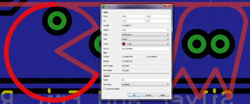
Once you've drawn an element out, you can always go back in there with the Info tool to manually adjust coordinates, widths, curves, and sizes.
For anything more complicated than basic shapes, though, you can import images using the bitmap import tool.
Import Bitmap
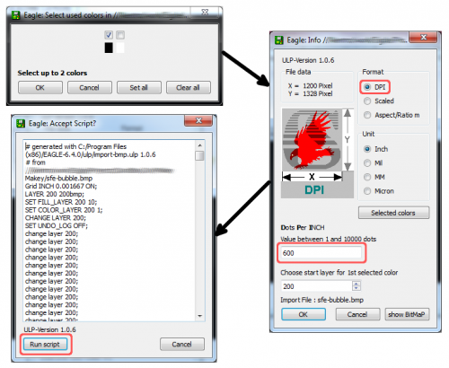
The import bitmap tool comes with all Eagle installs. Run it by going to File>Run ULP... and selecting import-bmp.ulp. Then select a bitmap (.bmp) file you'd like to import. Massage your bitmap before importing it, get rid of white space on the edges and save it into a monochrome format. That's ultimately what you're left with when it's imported onto a PCB: black or white, silk or no silk.
I use the (dots per inch) format when importing a bitmap. Measure out how big you want the image to physically be on the board, then divide that into the image's pixel-width.
A 1200 pixel image at 600 DPI would stretch the imported artwork out to 2 inches wide.
Place the image on an unused layer (like the 200 it defaults to), later you can Group it, and use the Change > Layer... tool to get it on the layer you need. Once you've got the scaling and layers set, OK that thing, and run the script it generates. It may take a few tries to get the image perfectly sized.
You can even use the import bitmap tool to add custom fonts, if you're not happy with either of the boring ones Eagle provides. This is what we did for the labels on the RedBoard:
Negative Silkscreen
One of the coolest effects you can add to your PCB design is inverse, or negative silkscreen. You can see this in action on the backside of an Arduino or in select sections of the MaKey MaKey.
There's no layer in Eagle that says "don't put silk here," so doing negative silk takes a little extra work. Fortunately, among a huge list of user-submitted scripts in CadSoft's database, there is a ULP called negasilk. It takes some experimentation to get right (check the negasilk.ulp file for full directions), but the result is well worth it. Silkscreen has a really nice, soft, shiny look to it, and it looks especially great in large chunks.
Final Checks
Finally, I like to get a good model of what my board is going to look like before I order it. Eagle can only get you so far...you can turn off all bottom layers or top layers at once to get an idea of what each side looks like, but it's still hard to visualize. My favorite tool for modeling an Eagle design is EagleUp.
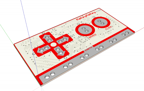
EagleUp is a really well done ULP/Sketchup plugin combo, which can get you a 3D model of your entire design (provided you have 3D models of every component...we're working on that, you can help!). It's great for visualizing just the PCB too; with minimal effort, you can get an accurate model like this:
Without this EagleUp model, we'd never have realized how hokey those stars looked.
Pretty close to the real thing! With that you can go back and change whatever looks funny, or pull the trigger and send your gerbers off to the fab house. Woo!
What About You?
I'd love to hear about what secrets you've gleaned. Anything I've missed? Care to share some of your PCB artwork? We do all of our PCB design in Eagle, so forgive me for ignoring some of the other great design tools out there. Do any of those make PCB art easier?

Thanks for sharing! I always liked the 'vanity pcbs' such as the DEFCON hacker conference batches. If you're into this, you might like this design which I recently did for a soldering workshop at ProtoSpace FabLab Utrecht, the Netherlands: Proto POV
Basically, it's a derivative of the Blinky POV by Wayne and Layne. More info (in Dutch) and the design is available at: Proto POV design
Note the golden QR code, and the ProtoSpace logo that's embedded under the solder mask in the copper layer (right bottom) on the back.
For the dimension layer, I used this tutorial, which is a nice addition to your collection of tips and tricks: From illustrator to Eagle
Wow. That is beautiful. The lettering,,,,
Who cares about the lettering, THE GOLD!!
NICE job! Loving the QR code and the lettering!
Jim is well-known around here for his absolutely beautiful boards (and writing). Thanks for sharing your secrets!
I hid a signature image in an internal layer once, right under the company logo silks. I left a window in the floods so you could see it with a back-light.
Cool
I say, if you have logos and similar things already in vector format (such as in Illustrator) you should just skip doing the route of the import bitmap. Instead, save it out as a DXF file and import it using one of the many scripts to turn DXF into usable Eagle polygons. Generates a much better result in my experience.
While I find purposefully artistic boards are interesting, I think you guys are missing the reality that a properly placed and routed board is in itself art. I've been doing this stuff much longer than I care to admit. And it now takes me a few seconds to look at a board and understand if the layout was done by a hack or an "artist".
Excellent point! All Sparkfun boards are reviewed in front of all the engineers, and it's a tough room. Even without the above flourishes, Jim's boards are consistently works of art.
Yikes! The DPI setting in import-bmp controls something much more important than the scaled image size: It controls the size of the "pixels" that your image is drawn with, which in turn affects the end file size and could have consequences for manufacturability.
600DPI equates to 1.6 mil lines. If you're putting this in a silkscreen layer, well, chances are, the fab's silkscreen printer is basically 200DPI. Your image may or may not show up, depending on the fab's pre-processing process. This goes similarly with the soldermask layer (though the resolution is often higher).
The worst is if you try to put this on a copper layer. Each 1.6mil pixel is going to throw a "trace too small" warning in the fab's DRC software.
The moral: Be nice to your fab, and scale the image outside of import-bmp, so it processes well at 200DPI or smaller.
I did some experiments a while back to find what palette I could get using all combinations of mask/silk/copper. I found silk+copper(-mask) gives a slightly orange tinted white, and silk(-mask-copper) gives a slightly whiter white than silk+mask(-copper) on its own. Both of these looked flatter as well, as the solder mask adds an extra bit of height. Unfortunately silk alignment isn't always super precise, so it's more suited to larger things. The effect is quite subtle, really only visible when next to other uses of silk.
There's also exposing FR4 on both sides of the board, or exposing FR4 on one side, and silk or mask on the other, for varying degrees of "transparency". I have plans to use exposed FR4 as a light diffuser for an upcoming project.
I did (what I thought) was some pretty fun trickery to get a pattern in copper. Check out my instructable here.. http://www.instructables.com/id/ArduFlake-Turn-you-Arduino-into-the-best-gift-of-/
The hardest part was to get the image I wanted to not interfere with the traces... I wish when you imported graphics in eagle they were more polygon based rather than rasterized traces...
You know, I'm starting to really like the Enginursday posts. Kudos!
I personally also like aligning components in lines/shapes, not completely randomly, if possible. Logos, revision numbers, dates, and just general nerd cred easter eggs like google glass' >9k are also important.
I hate seeing a board with stuff placed randomly. Give it an order, no matter how complex. Need some nerd cred for my next board... Idk.. might do some star wars or ZORK
-------------------- Tech Support Tips/Troubleshooting/Common Issues --------------------
Since Autodesk obtained Eagle, the negasilk.ulp can be found here:
Here's an excellent GIF that shows how to do use the negasilk.ulp:
I managed to import an image of the Chinese dragon called Suanni, as that was our project name at work. Made some rather snazzy coasters that came out nice. Gold plated lettering on the front, Suanni and team member names on the back.
When importing an image into the copper layer, I like to draw the images on the keepout layer inversely, so that the image is created from a copper pour and I can get fine resolution without causing a lot minimum line width errors. See:
http://dboyer.us/electronics/complex-graphics-in-eagle
Just out of curiosity, does CadSoft Inc. give you guys anything for all the free advertisement SparkFun provides for them? And does anyone make pcb layout software for an android tablet?
I doubt it. And I wouldnt call it free advertising. Sure, Sparkfun mentions them a lot, but I've tried other CAD software and EAGLE is pretty dang powerful compared to them. Not to mention its licence isn't like $25,000. It's just what Sparkfun has chosen to work with, and its great for us because its freely available in a hobby version, so the general public can use their library, etc.
As for android CAD, I dont think there would be anything out there....
The free version of EagleCAD has a limited PCB size, but this can be circumvented ( to some degree ) by creating your own component footprints from geometric forms rather than using library components... that defeats a LOT of the desirable functions in EagleCAD because the footprints have no "identity" and must be copied manually from an original ( hand-carved ) footprint with group/cut/paste operations... but it will allow oversized PCBs to be saved... I've created PCBs as large as 12 x 12 inches using this ( crude ) "trick" with the free EagleCAD version. I've also used EagleCAD to create PCB panels that can be soldered together to make custom enclosures / boxes of exactly the right size and shape for my purpose, ( they look very slick ) with precise holes and cutouts for controls, indicators and connectors, and silkscreen legends for the panel controls. A bit pricey, but looks very professional when finished.
Can we see pics? :)
Recently I've been converting the sharp angles to smooth flowing curves and the electrons are thanking me for it...
This one * facebook link * is a socially interactive badge (IR + Arduino) for the Nuit Blanche Art Festival in November..
With photoshop you can manipulate bitmaps to make them more Eagle friendly by adding a hard mix layer with a halftone over your image. The dodge and burn tools can then be used to tweak the level of detail. Here's an example from a Data's head PCB that I've been working on http://i795.photobucket.com/albums/yy232/smolder_bucket/datashead.jpg. I also like using polygons for drawing since, unlike bitmaps, they can be routed through.
Just last week I got my Sparkman boards in the mail (dunna da da!) http://i795.photobucket.com/albums/yy232/smolder_bucket/DSCF3553.jpg.
Nice write-up. I can't use Eagle. For an old-timer Eagle does basically everything wrong from color scheme to what you click. (Doesn't everyone know that schematic signal lines are black?) I use Diptrace, which has a free version and is more in line with the Protel, OrCAD, Altium paradigm. My only regret is that Sparkfun publishes all the footprints in Eagle only.
It's easy enough to change the color scheme. One of EAGLE's strengths (and weaknesses) is the incredible degree to which it can be customized.
I'm colorblind and impatient, and my EAGLE shortcut keys and colors are different to everyone else's around here. But it works for me!
Thank you!
Made this one a long time ago as a proof of concept more than anything: MLP:Twilight
AutoCAD with an in-house Eagle exporter (the DXF importer ULP was horribly broken). Not a valid board, though, and some of the colors would be difficult to attain on an actual board :)
Eagle itself would be tons nicer if it supported splines (bezier,b-,or any other really) rather than just the limited straight lines and arcs. And PCBs would be tons nicer if we could have full color silkscreens.. at least once the novelty wears off and all the Geocities/Myspace-inspired boards were done ;)
Were using Eagle ... now using a more expensive one, I can visualize PCB in 3D, integrate it to the box/case, and can route boards like 10x faster. You always get what you paid for it seems ;)
one of the main reasons we still use Eagle is because it can be had for free. So by sharing our board designs, anyone can easily have access to them for their own modification or just learning how it was done. We never said it was the best tool out there, it's just very accessible for our customers.
What by chance is more powerful than EAGLE? I mean, EAGLE is great for my needs (small boards and DIY stuff), but if I ever go further, how much $$$ am I looking at for a licence of this stuff?
Well, the ''minimal upgrade, Light version'', just so you can use it commercially, is not that expensive at ~$60 apiece (according to last year's prices). The next step up is I think the ''standard version'', which allows 4 signal layers, a much larger board area, and so on, and you can check how much it costs if you go to Cadsoft's site, and try purchasing. Make sure you get the right version; files made in v5.0 are incompatible with v6.0.
Just checked some on CADSOFT's site. A licence for the 6 layer (next step up from the light version) is like $820, but the student discount is like $410. For the professional stuff (16 layer, 4x4m board size) is $1640 for one licence, and $820 for a student. :O :O
Why, Mister Anderson, why do you Persist?
Whoa. Never realized how much it was. The lite version should work for most small companies, however. A part of me giggles at the 4*4m board size. Never send a man to do a machine's job.
Yeah its pretty darn expensive. Not as bad as a MasterCAM licence (machining software...), but consider the adobe software you could get with that! I believe though, that the lite version limits you to a 100x80mm routing area. Not that much (like a 3x4 inch area). Great for small boards or Arduino shields, but anything more than that and you're either looking for a different CAD software or a better paying job :)
I would love to see a 4x4m Arduino.... Good luck finding a manufacturer that does that size though!!
You're the one, Neo
Or Solidworks, or, (sputter) Autodesk Inventor. Yeah, the lite version limits you, but I've found that 4*4in is actually very large. You can really do a lot in that space. And, I've tried several other popular PCB design programs, and have always settles on Eagle. The $800 prices aren't really that expensive in the field. While it might be pricey compared to FreePCB and such, it's cheap compared to (cough)Altium(wheeze).
Fasten your seatbelt, cuz we ain't in Kansas no more. (Cmon, Cypher! We all know one does not negotiate with a Smith!)